Adam Harsant, MD provides some valuable technical insights into choosing the right reflow process for your PCB Assembly. The reflow process stands as a cornerstone in the realm of PCB assembly, playing a pivotal role in the creation of reliable and high-quality electronic assemblies.
Following the solder paste printing and component placement, reflow is crucial for ensuring reliable, high-quality PCB assemblies. Reflow subjects the assembled PCB to carefully controlled heating cycles to achieve the correct metallic bond. Beyond mere soldering, reflow encapsulates the essence of quality assurance, ensuring that each PCB emerges as a robust, reliable entity capable of meeting stringent performance standards.
Over the years, various reflow methods have emerged, each addressing specific technological demands and product requirements, such as greater accuracy with tighter process windows.
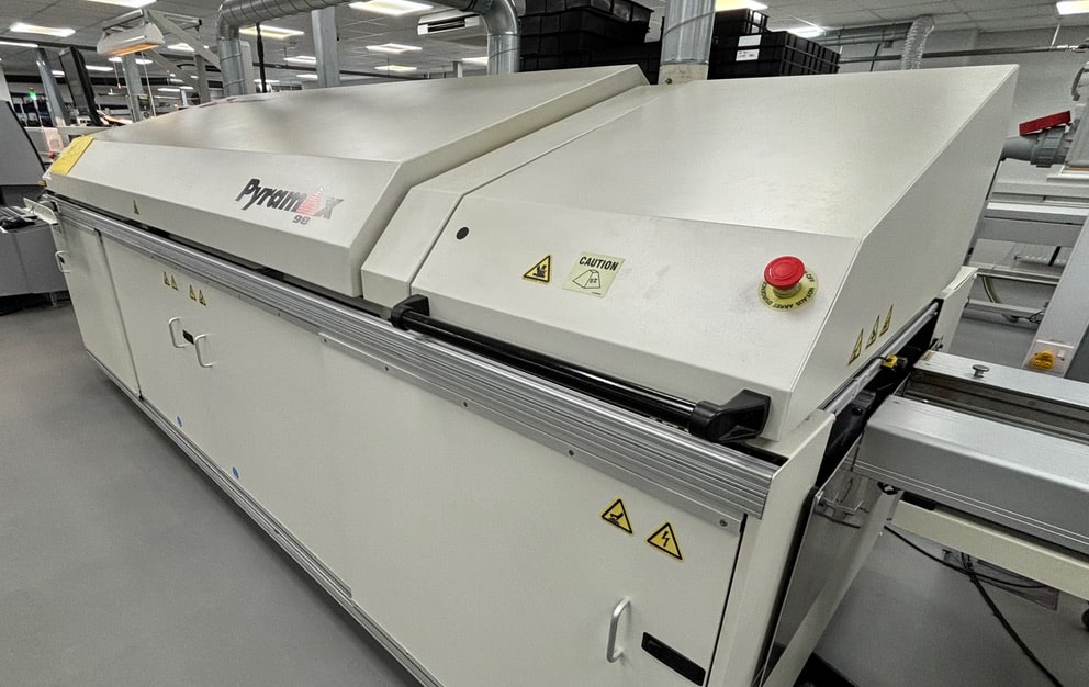
The established go-to reflow process has been convection reflow, which still stands today as a robust reflow method and is widely used here at TechPoint Solutions Ltd (Formerly
To achieve such joint integrity, we select the best-fit process for our customer’s product. Working with convection, vapour phase reflow, vacuum vapour phase, and Nitrogen (N2) reflow affords us this luxury.
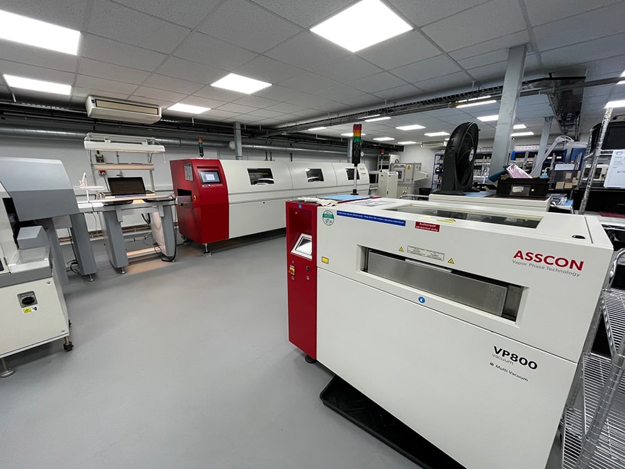
TechPoint Solutions Ltd (Formerly
Using Asscon process technology and Golden as a heat transfer medium which limits the chemical exchange to a maximum temperature of 240dc, ensuring the PCBA can evenly absorb heat until every component has been reflowed without exceeding this temperature and causing overheating to any component.
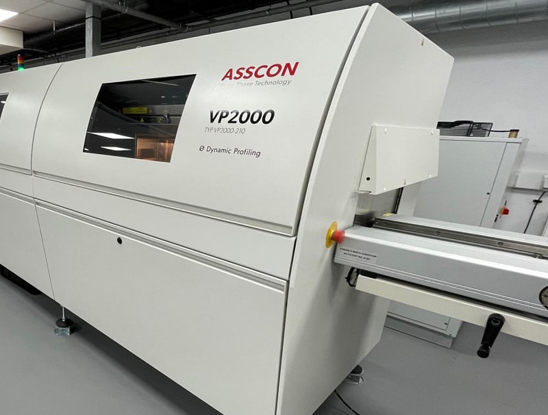
Adding vacuum technology to support our aerospace customers sets the standard even higher by allowing us to remove oxygen within the solder paste that contributes to voiding – all of which can be validated under X-Ray at TechPoint Solutions Ltd (Formerly
Should the PCB feature component features that require the use of type 6 & 7 solder paste due to small pad features and/or narrow process windows, then liquid Nitrogen (N2) can be used in our ERSA Hotflow oven to ensure a fully inert atmosphere is achieved and once again increase joint integrity.
All our ovens are equipped with onboard profile management tools and supported by data loggers so that our engineers can calculate the correct thermal profile to suit our customers’ products. Our sitewide MES system binds all the process parameters and technical data to provide a fully traceable path of engineering processes and controls, ensuring a vast amount of knowledge can be transferred for review and process improvements.
The process controls within TechPoint Solutions Ltd (Formerly
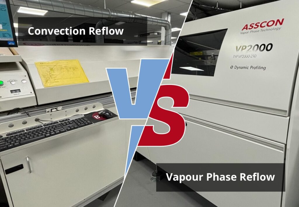
Now that we’ve established the critical importance of the reflow process in PCB assembly, let’s explore two prominent methods that have revolutionised soldering techniques: convection reflow, and vapour phase reflow. Each method brings unique advantages and considerations to the table, addressing the evolving technological demands and product requirements of modern electronics manufacturing.
Convection Reflow
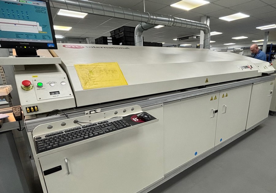
Convection reflow remains a stalwart in PCB assembly due to its reliability and versatility. Widely employed across different industries, it ensures product conformance and integrity, paving the way for downstream processes. This method is well-suited for a diverse range of component types, including surface-mount devices (SMDs), through-hole components, and even complex multi-layer boards. This versatility extends to its compatibility with various solder pastes, including lead-free formulations, ensuring compliance with environmental regulations and industry standards.
Moreover, the convection process minimises thermal stress on sensitive components, reducing the risk of defects such as tombstoning or solder voids. This capability enhances the overall reliability of the assembly, crucial for applications demanding high performance and longevity.
Additionally, convection reflow offers consistent and repeatable results, making it ideal for high-volume production environments. Its precise temperature control and uniform heating distribution across the PCB surface ensure product conformance and integrity, paving the way for downstream processes with minimal rework or reject rates.
Typically, the convection method consists of four heat phases: preheating, thermal soaking, reflow and cooling. These phases are depicted as a series of zones within the convection oven, each with independently controlled temperature settings, where the PCB passes through on a conveyor belt. The arrangement of these zones plays a critical role in achieving a precise and uniform temperature profile throughout the reflow process.
The Convection Reflow Process:
Zone 1, Preheating Zone: Gradually raises the PCB temperature to prevent thermal shock, ideally at 1-3°C per second. This process helps prevent thermal shock, which could damage sensitive components. The rate at which the temperature increases in this zone is crucial, as too rapid heating could cause component warping, while too slow heating could lead to solder paste drying. An ideal preheat rate is between 1 and 3°C per second.
Zone 2, Thermal Soaking Zone: Ensures uniform temperature, activating flux in the solder paste and removing oxides from the surfaces to be soldered. The soaking zone is vital for achieving consistent solder joint quality, as it helps minimise temperature variations across the PCB assembly.
Zone 3, Reflow Zone: Melts the solder paste, forming strong metallurgical bonds between the component leads and the PCB pads at peak temperatures of 235-250°C. Maintaining this temperature within a specified range and duration is essential to ensure optimal solder joint formation without damaging components or causing other solder-related defects.
Zone 4, Cooling Zone: Rapidly solidifies solder joints to prevent intermetallic compound formation that could weaken the solder connection, ideally at 2-4°C per second. Too rapid cooling can cause thermal soak, while too slow cooling can lead to the formation of brittle solder joints. An ideal cooling rate is between 2 and 4°C per second.
The number of zones in a reflow oven can vary depending on the specific model and manufacturer. More advanced reflow ovens may have additional zones or sub-zones for fine-tuning the temperature profile, providing increased process control over the reflow process and ensuring consistent solder joint quality.
As the convection process is ‘in line’ with the rest of the assembly process, greater throughput can be achieved because it integrates with the other SMT systems, automating the entire process.
Advantages of Convection Reflow:
Reliable Product Quality: Convection reflow provides consistent and high-quality solder joints due to precise temperature control. However, vapor phase reflow also ensures high-quality joints with better wetting due to its inert atmosphere.
Enhanced Durability: Convection reflow can produce durable assemblies, but vapor phase reflow is particularly effective at avoiding overheating and ensuring uniform heating, which can further enhance durability.
Flexibility for Complex Designs: Convection reflow is suitable for a wide range of PCB designs, but vapour phase reflow excels in handling boards with diverse thermal mass components, ensuring minimal temperature fluctuations.
Cost-Effective Solutions: Convection reflow is typically more cost-effective for high-volume production due to its in-line process integration. Vapour phase reflow, while providing superior control and quality for certain applications, tends to be more expensive and less suited for high-volume continuous production.
Consistent Performance: Convection reflow provides reliable performance, but the inert atmosphere in vapour phase reflow significantly reduces voiding in solder joints, which can result in even higher reliability for critical applications.
Improved Product Reliability: Convection reflow provides thorough process control and traceability, ensuring reliable products. Vapour phase reflow offers exceptional reliability for complex boards, especially in critical applications where avoiding overheating is crucial.
Vapour Phase Reflow
Vapour phase reflow addresses one of the most significant challenges in PCB assembly: achieving uniform heat distribution during soldering. As PCBs become increasingly complex with components of varying sizes and thermal requirements, traditional soldering methods often struggle to deliver consistent results.
In vapour phase reflow, an inert liquid is heated to create a controlled vapour atmosphere within a specialised oven. This vapour envelopes the PCB, ensuring that all components receive uniform heating, regardless of their size or position on the board. This unique heating method gives more control, providing the ability to alter the temperatures and so eliminating the risk of overheating or thermal gradients, preserving the integrity of delicate components and preventing solder defects.
Moreover, vapour phase reflow offers unparalleled control over the soldering process. Operators can precisely adjust the temperature within the vapour phase reflow oven, accommodating different solder pastes and meeting the specific requirements of each PCB assembly. This precision not only enhances product quality but also minimises the need for rework, leading to higher overall efficiency.
Furthermore, vapour phase reflow is particularly advantageous for sensitive components or assemblies requiring high reliability. Its gentle heating process minimises thermal stress, prolonging the lifespan of electronic devices and ensuring consistent performance over time.
The versatility and efficiency of vapour phase reflow makes it a preferred choice for demanding applications across industries such as aerospace, automotive, and medical devices.
The Vapour Phase Reflow Process:
Fluid Evaporation: The process begins by heating a specialized perfluoropolyether fluid (PFPE) until it evaporates.
Vapour Formation: A dense layer of vapour forms, filling the oven chamber. This creates an inert, oxygen-free atmosphere, which is crucial for preventing oxidation during the reflow process.
Protective Gas Atmosphere: The vapour, being heavier than the surrounding air, forms a protective layer over the PCB assembly (PCBA), ensuring consistent heat distribution and protecting components from oxidation.
Heat Transfer: The PCB, along with its components, is placed on a tray and lowered into the vapour zone. As the vapour condenses on the PCB, heat is transferred efficiently and uniformly across the assembly.
Thermal Exchange: The PCB and solder paste reach the same temperature as the vapour. The heat melts the solder paste, forming strong metallurgical bonds between the components and the PCB pads. This phase avoids aggressive temperature changes, allowing for a gradual and controlled reflow process.
Cooling and Solidification: Once the solder paste has melted and the components are securely joined, the PCB needs to cool to solidify the solder joints. Cooling elements in the oven assist in this process, ensuring the paste hardens properly. The tray is then lifted out of the oven, completing the reflow process.
Advantages of Vapour Phase Reflow:
Board & Component Integrity Maintained: The vapour phase reflow process prevents the PCB and its components from overheating, maintaining the integrity of all elements. This ensures the board will not bend or break during the process. In contrast, while convection reflow also aims to prevent overheating, the direct heat application can sometimes pose a higher risk of thermal damage, especially for delicate components.
Temperature Consistency: The inert atmosphere of the vapour phase method ensures consistent temperatures and efficient wetting of the solder paste. Overheating is eliminated as the temperature is limited to the maximum temperature of the vapour, around 230°C for lead-free soldering. Additionally, engineers can control oven temperature as needed. Convection reflow also provides good temperature control, but may experience more temperature variations due to the direct air heating method.
Minimal Temperature Fluctuations: This method is particularly effective for PCBs with components of varying thermal mass. It minimises temperature fluctuations between different components, ensuring uniform reflow and reducing the risk of thermal damage. With no shadowing between large and small components, heat is evenly distributed across the board, ensuring all components adhere simultaneously regardless of size. Convection reflow, while effective, can sometimes struggle with uniform heat distribution, particularly on densely populated boards with mixed component sizes.
Improves Wetting with Oxidation Prevention: The inert atmosphere in the vapour phase reflow process removes oxygen from the chamber. Without oxygen, the vapour creates better wetting of the PCBs, resulting in high-quality solder joints. Convection reflow, although effective, does not inherently provide an oxygen-free environment, which can sometimes lead to oxidation issues and reduced solder joint quality.
Versatility: Vapour phase reflow is suitable for various products, including flex, flex-rigid, heavy-mass copper, and complex high-layer-count PCB substrates. While convection reflow is versatile and suitable for a broad range of designs, it might not handle the thermal mass variations and complex structures as effectively as vapour phase reflow.
Scale & Throughput: TechPoint Solutions Ltd (Formerly
At a Glance Comparison
Convection Reflow:
Cost-Effective for High Volume: Ideal for large-scale production with lower operational costs compared to vapor phase reflow.
Wide Applicability: Suitable for a broad range of PCB designs, including those with varying component sizes.
Scalability: Easily scales to meet varying production volumes, ensuring flexibility for customer demand.
Reliable Solder Joints: Ensures consistent solder joint quality with precise temperature control.
Good Process Control: Provides detailed control over the reflow process, ensuring high-quality outputs.
Vapour Phase Reflow:
Superior Temperature Control: Provides uniform heating with minimal temperature fluctuations, ideal for complex PCBs.
Inert Atmosphere: Ensures better wetting and significantly reduces voiding in solder joints.
Prevents Overheating: The maximum temperature of the vapor prevents overheating of the PCB and components.
Enhanced Durability: Provides exceptional reliability, particularly for critical applications in aerospace, defence, and medical fields.
Ideal for Complex Designs: Excels in handling boards with diverse thermal mass components.
High-Quality Solder Joints: Produces joints with high integrity and reliability due to the controlled environment.
High-Throughput: When using a fully automtated in-line system, such as the Asscon VP2000 used at TechPoint Solutions Ltd (Formerly
Reduced Production Time: Shorter lead times and quicker delivery enhance time-to-market capabilities.