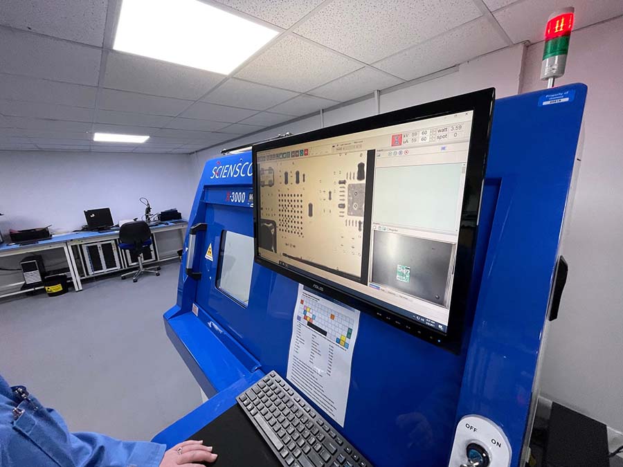
Gemini Tec add the latest Scienscope X-Scope 3000 X-Ray system to its QA department for 2020.Advanced X-Ray with Scienscope
Our latest investment provides additional capability and capacity for PCBA inspection to support our customers production of PCBA’s
This latest system is packed with advanced features for the inspection and validation of products. Using a powerful 130kV high power micro power focused closed tube X-Ray source to inspect a wide variety of electronic components beyond BGA & QFN devices, including inner layer PCBs, over moulded connectors, encapsulated connectors, aluminium die castings, wire bonding and semiconductors.
Advanced software tools provide features such as automatic void detection on every electronic component post reflow. Automatic programming now allows us to define the exact devices that require X-ray inspection and subsequently enact the program using the PCBA bar code during the various stages of the production.
Reporting to customers will now be further enhanced with the provision of custom data being produced for any PCBA being manufactured. The advanced software features of the Scienscope X-Scope 3000 provide detailed analysis such as exact measurements for BGA ball sizes and evidence of voiding within the limits of acceptability. Such reports will feature within our standard FAIR reports.
The machine has a large working inspection area of 595mm x 460mm, to cover large back planes, inspecting oblique angles of ±50°.
Adding the latest feature rich Scienscope X-Scope 3000 X-Ray into our QA department compliments our current X-Ray capability with our X-Tek system and also drives forward our capability to support customers further with complex PCBA hardware.
The system becomes fully operational in September 2020 and is forms part of a much wider expansion at Gemini Tec to increase support for its customers and ensure capacity for new customers who are eager to benefit from a UK CEM service.