Gemini Tec are pleased to announce its latest expansion plans for 2020, with the addition of a further 10,000 sqft facility. Despite the current wider economic situation, Gemini Tec remain well positioned to expand its service and extend production capability to meet the rise in demand for advanced PCBA manufacturing in the UK. New Operations Centre At Gemini Tec Ltd
This latest move provides a substantial increase in our production footprint, which will house our latest investment in Mycronic SMT equipment, comprising of 2 new SMT machines to create a new ‘ultra’ high mix surface mount line.
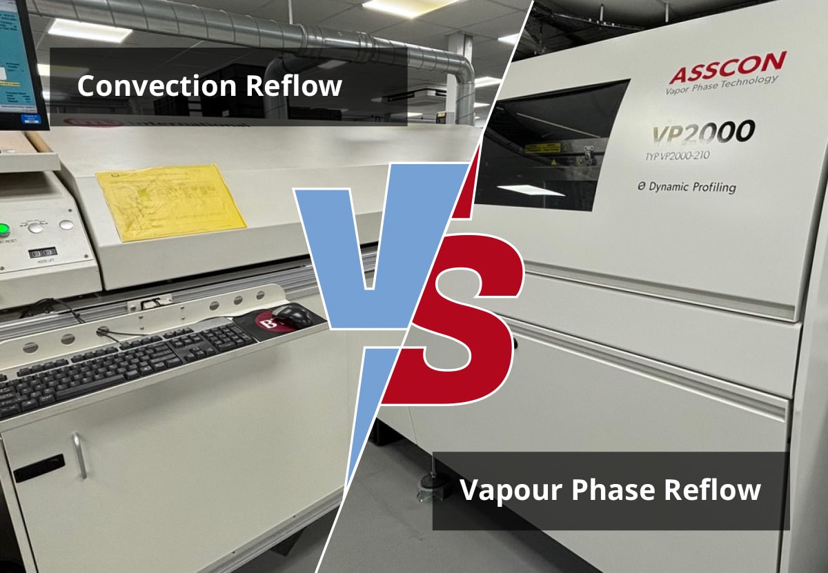
Our latest SMT line has been configured for higher volume and high mix products, complete with fully automatic line loading and fully automatic conveyors. Our latest surface mount line will be using solder jet printing and vapour phase reflow, in keeping with our wider strategy. However N2 reflow technology will also be integrated in Q1/2021.
The additional space expands our PCB assembly and box build area to undertake a new major contract from our automotive customer and ensure ample room for growth in new business.
A new operations centre will bring together its commercial, engineering and procurement functions along with a purpose built ESD material kitting and product stocking facility.
The move is part of a planned expansion for Gemini Tec, allowing us to better support new customers with complex PCB hardware, using our unique blend of advanced capability from solder jet printing, N2 & vapour phase reflow with 3D AOI tools.
Our manufacturing capability is amongst the very best available within the UK, supporting customers in a broad range of market sectors, from automotive, RF to advanced telecoms equipment. Recent investment in technology includes advanced X-ray using Scienscope hardware for automatic void detection and 3D AOI, for advanced defect detection. Gemini Tec are perfectly poised to provide its services for complex and demanding products.